Si-based Resonant Interband Tunnel Diodes for Quantum Functional and Multi-level Circuitry (Mixed-Signal, Logic, and Low Power Embedded Memory) to Extend CMOS by Prof. Paul R. Berger

The EDS Germany Chapter and NanoP proudly presents Paul R. Berger from Ohio State University, USA for a Distinguished Lecture on “Si-based Resonant Interband Tunnel Diodes for Quantum Functional and Multi-level Circuitry (Mixed-Signal, Logic, and Low Power Embedded Memory) to Extend CMOS”. The lecture will be held on 22nd June 2023 at 2pm Berlin time. The Distiguished Lecture will be held on site (Werner-Hartmann-Bau, Room 205/206 , Nöthnitzer Str. 66 , 01187 Dresden ). Information provided via IEEE vTools by the following link: https://events.vtools.ieee.org/m/364569

Abstract:
The dawn of tunnel diodes, commonly attributed to Leo Esaki in the late 1950’s, predates much of the innovation and infrastructure investment into CMOS technology. But, the lack of a mass production process and inability to monolithically integrate these devices into complex circuits paved the way for the CMOS juggernaut seen today.

However, the unique negative differential resistance (NDR) systemic to all tunnel diodes provides a pathway to exploit new hybrid-CMOS circuit topologies with compact latches and reduced power consumption that could mitigate some of the bottlenecks perceived for scaled CMOS. A new paradigm of computing is possible, capitalizing upon transistor/tunnel diode integration if a viable Si-based tunnel diode could be developed. This talk will explore these opportunities.

This talk will provide a background on Si-based tunnel diode devices and circuits and summarize the results of Si-based RITD device optimization, their monolithic integration with Si-based transistors and present a range of circuit prototyping. The extension of NDR to ultra-low voltage memory will also be discussed.

Paul R. Berger Biography (S’84 M’91 SM’97 F’11):
Paul R. Berger
is a Professor in Electrical & Computer Engineering at Ohio State University and Physics (by Courtesy). He is also a Distinguished Visiting Professor at Tampere University in Finland. He received the B.S.E. in engineering physics, and the M.S.E. and Ph.D. (1990) in electrical engineering, respectively, all from the University of Michigan, Ann Arbor. Currently, Dr. Berger is actively working on quantum tunneling devices, printable semiconductor devices & circuits for IoT, bioelectronics, novel devices, novel semiconductors and applied physics.

Formerly, he worked at Bell Laboratories, Murray Hill, NJ (1990-’92) and taught at the University of Delaware in Electrical and Computer Engineering (1992-2000). In 1999, Prof. Berger took a sabbatical leave while working first at the Max-Planck Institute for Polymer Research, Mainz, Germany and then moved on to Cambridge Display Technology, Ltd., Cambridge, United Kingdom. In 2008, Prof. Berger spent an extended sabbatical leave at IMEC (Interuniversity Microelectronics Center) in Leuven, Belgium. Prof. Berger was also a Finnish Distinguished Professor (FiDiPro) at Tampere University of Technology (2014-2019), and he continued as a Fulbright-Nokia Distinguished Chair in Information and Communications Technologies (2020-2022) with the newly merged Tampere University.

He has authored over ~250 referred publications and presentations with another ~115 plenary, keynote, panelist, invited talks, 5 book sections and been issued 25 patents with a Google Scholar H-index of 37. Some notable recognitions for Dr. Berger were an NSF CAREER Award (1996), a DARPA ULTRA Sustained Excellence Award (1998), a Faculty Diversity Excellence Award (2009), Outstanding Engineering Educator for State of Ohio (2014), and IEEE Region-2’s Outstanding Engineering Educator Award (2023). He has been on the Program and Advisory Committees of numerous conferences, including the IEDM, EDTM, IFETC, DRC, EMC, ISDRS, CSTIC, CPTIC and IFSOE meetings. More recently Berger was General Chair the 2021 International Flexible Electronics Technology Conference (IFETC) meeting and was selected as the Founding Editor-in-Chief for the IEEE Journal on Flexible Electronics.

He currently is the Vice Chair of IEEE Columbus, which won the 2022 Best Chapter award (Medium-sized); Chair of the Columbus IEEE EDS/Photonics Chapter; and an IEEE Faculty Advisor for over 30 years. In addition, he is an elected member-at-large to the IEEE EDS Board of Governors (19’-24’), where he was the seminal Vice President of Strategic Directions (20’-21’) and now Chair of the Ad Hoc EDS Future Directions Committee (22’-23’). Berger is on the Steering Committees of the IEEE Future Directions communities, Brain and Quantum. Berger is also an EDS Representative to the IEEE Diversity and Inclusion Committee (2022); IEEE TAB Ad Hoc Climate Change Committee (2022-2023), and a member of the Women in EDS Committee (2022-2023).

He is an IEEE EDS Fellow (2011) and Distinguished Lecturer (since 2011), as well as a Senior member of the Optical Society of America. He has received >$10.2M in USA funding as lead PI, with an additional >$26.2M as Co-PI in USA and >€15.7M in funding from Finland and the European Union. Altogether, he has received ~$52.7M in research funding.

75 Years of the Transistor by Prof. Cor Claeys

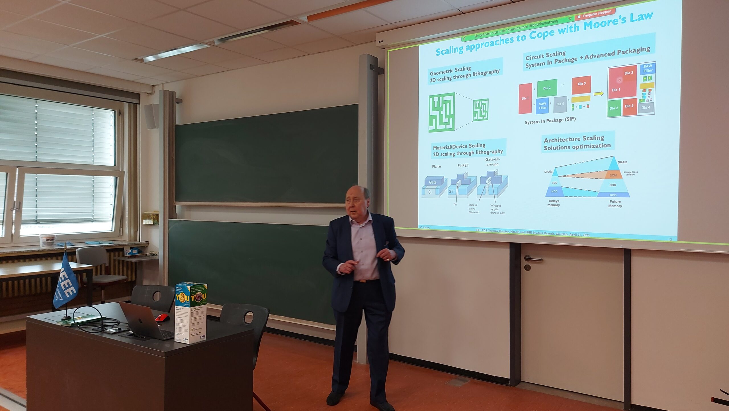
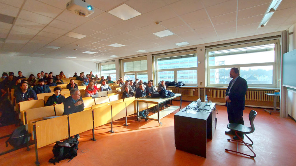
The EDS Germany Chapter organized a hybrid distinguished lecture entitled “Memories from Storage to Computing” on April21, 2023. The lecture was given by Prof. Cor Claeys from KU Leuven, IEEE Fellow, and was organized by Prof. Alexander Kloes and Prof. Mike Schwarz fromthe Competence Center for Nanotechnology and Photonics (NanoP) of THM – University of Applied Sciences, Germany.The DL was attended by 26 IEEE participants, as well as 56 non IEEE members onsite and via Zoom videoconference system.

Prof. Cor Claeys and Prof. Benjamin Iniguez celebrating the 75 anniversary of the transistor in front of the audience.

After a warm welcome ofProf.Schwarz, Prof. Claeys started with an evolutionary overview of the microelectronics history. Afterwards, actual numbers and examples of the invests of new waferfabs were given and supported by the evolution of 300mm fabs over the last decades. Prof. Claeys highlighted the different aspects of waferfab investment and it occurring management to make revenue. From that point of view more details in scaling approaches to cope Moore’s Law where presented with its different implications of technology. These focus finally in advance silicon devices from planar FET to Stacked Nanosheet (NS) and approaches like Forksheet (FSH).

Afterwards, Prof.Claeys gave insights in Germanium devices and its most important challenge: Defects. He referred to the stacks of Germanium devices to control defects, gave some examples on the feasibility of Ge-Technology at device level and many famous examples. Then next topic focused on III-V on Silicon with it aspects on lattice mismatch, resulting defects and measures to improves device performances. Many examples of state-of-art devices were given.  A comparison was between the progress  in GaN and SiC was also discussed.

Prof. Cor Claeys during his lecture 75 Years of the Transistor – Trends and Challenges in Micro- and Nanoelectronics for the Next Decade.

Finally, Prof. Claeys offered the impact of increased system functionality and density achieved by 3D integration based on Through Silicon Vias (TSV) and/or monolithic or 3D sequential integration on a Si substrate. He discussed the evolution, trends and challenges imposed on materials and devices for different integration technologies.

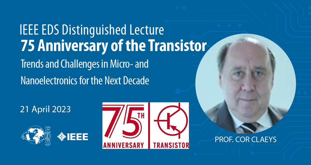
75 Years of the Transistor – Trends and Challenges in Micro- and Nanoelectronics for the Next Decade by Prof. Cor Claeys

The EDS Germany Chapter and NanoP proudly presents Cor Claeys from KU Leuven, Belgium for a Distinguished Lecture on “75 Years of the Transistor – Trends and Challenges in Micro- and Nanoelectronics for the Next Decade”. The lecture will be held on 21st April 2023 at 2pm Berlin time. The Distiguished Lecture will be held in hybrid format, on site (TH Mittelhessen, Wiesenstraße 14, 35390 Gießen, Building A10, Room 6.20) and via Zoom. Login information provided before the event and requires registration. Interest participants please register via IEEE vTools by the following link: https://meetings.vtools.ieee.org/m/346991


Abstract:
Semiconductor technology knowns an exponential evolution in the last decades and is fully integrated in our everyday life. According to the Semiconductor Industry association (SIA) the global semiconductor industry sales reaches US$ 600 billion in 2022, corresponding with a shipment of more than 1.2 trillion components. This necessitated implementation of many novel materials, advanced design concepts and new transistor structures. Increased device performance and reduced power consumption, while maintaining a good manufacturability and yield performance without penalizing the cost/function, are driving microelectronic research towards 3-nm technologies. A large variety of device architectures such as FinFETs, TFETs, negative capacitance, Gate-All-Around, nanowires (NWs), nanosheets (NSs) in both horizontal or vertical configurations, CFET and Forksheet structures are extensively investigated for both logic and analog/RF building blocks enabling System-on-Chip (SoC) applications. Innovative heterogeneous Ge and III-V technologies on a Si platform are also gaining interest. Wide bandgap materials such as III-nitrides have a strong potential for RF and power parts. Increased system functionality and density is achieved by 3D integration based on Through Silicon Vias (TSV) and/or monolithic or 3D sequential integration on a Si substrate. The evolution, trends and challenges imposed on materials and devices are discussed for different integration technologies.

Cor Claeys Biography:
Cor Claeys is Professor at the KU Leuven (Belgium) since 1990. He was with imec, Leuven, Belgium from 1984 till 2016 and had different positions including, including and Director Strategic Relations. His main interests are semiconductor technology, device physics, low frequency noise phenomena, radiation effects and defect engineering. He is teaching a variety of short courses in different parts of the world (Europe, China, India and Brazil).

He co-edited books on “Low Temperature Electronics” and “Germanium-Based Technologies: From Materials to Devices” and wrote monographs on “Radiation Effects in Advanced Semiconductor Materials and Devices”, “Fundamental and Technological Aspects of Extended Defects in Germanium”, “Random Telegraph Signals in Semiconductor Devices” and “Metals in Silicon- and Germanium-Based Technologies: Origin, Characterization, Control and Electrical Impact”. Two books are translated in Chinese. He (co)authored 16 book chapters, over 1200 conference presentations and more than 1400 technical papers (of which more than 430 in peer-reviewed scientific journal). He is editor/co-editor of 70 Conference Proceedings.

Prof. Claeys has been the project investigator of a large variety of both European and bilateral research projects with industrial partners related to silicon technology, device physics and device applications for space activities and internet of things (e.g. infrared detectors, retina sensor, CCDs for medical applications etc.). Several international projects have been dealing with low frequency noise characterization of advanced semiconductor devices.

Prof. Claeys is a Fellow of the Electrochemical Society and of IEEE. He was Founder of the IEEE Electron Devices Benelux Chapter, Chair of the IEEE Benelux Section, elected Board of Governors Member and EDS Vice President for Chapters and Regions. He was EDS President in 2008-2009 and Division Director on the IEEE Board of Directors in 2012-2013. He is a recipient of the IEEE Third Millennium Medal and received the IEEE EDS Distinguished Service Award. He is a Distinguished Lecture of the IEEE Electron Devices Society. Within the Electrochemical Society, he was Chair of the Electronics & Photonics Division (2001-2003) . In 2004, he received the Electronics & Photonics Division Award. In 2016 he received the Semi China Special Recognition Award for outstanding involvement in the China Semiconductor Technology International Conference (CSTIC).

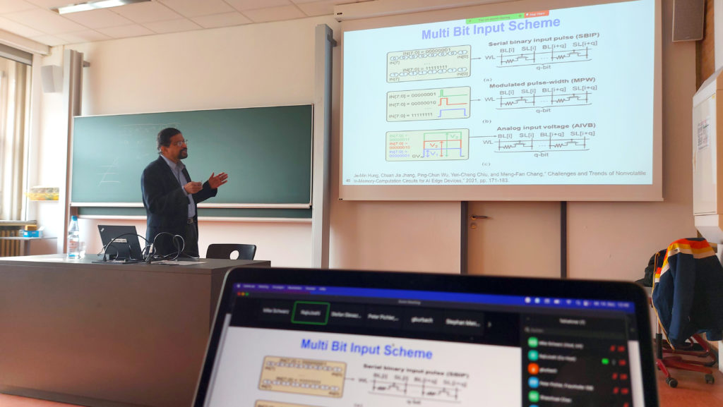
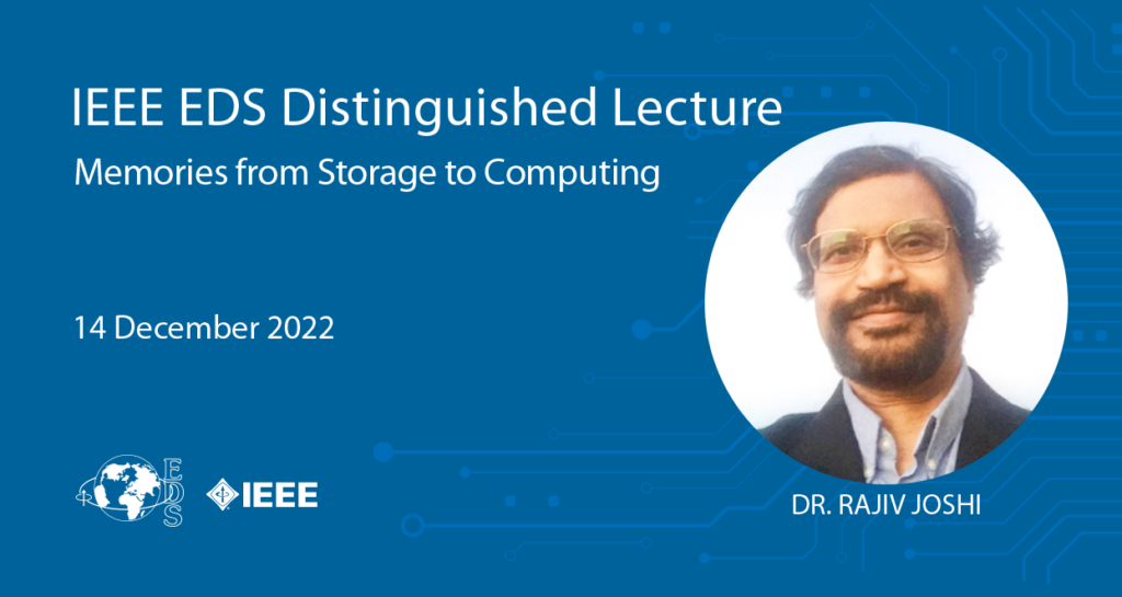
Rajiv Joshi presented “Memories from Storage to Computing”

The EDS Germany Chapter organized a hybrid distinguished lecture entitled “Memories from Storage to Computing” on December 14, 2022. The lecture was given by Dr. Rajiv Joshi from IBM – T. J. Watson Research Center, IEEE Fellow, and was organized by Prof. Alexander Kloes and Prof. Mike Schwarz from the Competence Center for Nanotechnology and Photonics (NanoP) of THM – University of Applied Sciences, Germany. The DL was attended by 17 IEEE participants, as well as 43 non IEEE members onsite and via Zoom videoconference system.

After a welcome from Prof. Schwarz, Dr. Joshi stepped directly into the subject of memories. A comprehensive introduction with the essential basics was part of the first minutes of the DL. The first semester’s students welcomed the context Dr. Joshi presented, and found many theoretical discussed topics of microcomputer technology lectures in practical applications.

Then the lecture concentrated on the brick wall of memories, focusing on the memory bandwidth wall. The outcome of the brick wall challenge, postulated back in the past by Dr. David Patterson, was that all components i.e. power wall, memory wall and ILP (instruction level parallelism) wall sum up. From that point of view the need and/or push for low Vmin was obvious during the following discussions. Finally, power dissipation and further attributes play a significant role in memories. Designers have to deal with all the attributes (non-volatility, high density, low power consumption, bit alterability, endurance, low cost, etc.) and there is always an engineering tradeoff and no holy grail for memories.

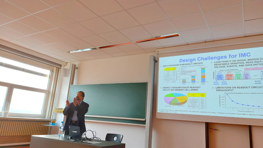
Dr. Joshi went through the topic of memory as storage and discussed SRAMs as storage and methods like boosting during read out to stabilize the cells. Afterwards, the impact of variability and considering this domain during designing was addressed. The demand on fast algorithms to explore the tails of statistical variability distributions is required to ensure high yields. After this part of the lecture Dr. Joshi changed the focus on “From Moore´s law to AI law”. Within this part various discussions on i.e. the explosion of alternative processing power (CPU à GPU à NPU) took place. Furthermore, deep learning and enhancing its performance was under consideration by considering building blocks of those and realize them in hardware to allow for computation with memory. Finally, non-volatile memory technologies were compared by experimental data and the design challenges of InMemory Computing (IMC) concluded an excellent distinguished lecture. This was finished by high level QnA after the lecture. The students particularly liked the conceptual presentation of the basics and the continuous increase in level up to the advanced topics. Finally, it was a very well mixture of low and advanced level topics.

Rajiv Joshi Distinguished Lecture on 14th December 2022

The EDS Germany Chapter and NanoP proudly presents Rajiv Joshi from IBM, T. J. Watson Research Center, US for a Distinguished Lecture on “Memories from Storage to Computing”. The lecture will be held on 14th December 2022 at 12am Berlin time. The Distiguished Lecture will be held in hybrid format, on site (TH Mittelhessen, Wiesenstraße 14, 35390 Gießen, Building A10, Room 6.20) and via Zoom. Login information provided before the event and requires registration. Interest participants please register via IEEE vTools by the following link: https://meetings.vtools.ieee.org/m/333022

Abstract:
Volatile (VM) and nonvolatile memories (NVM) are key to the electronic industry. The growth is attributed to growing computing capabilities with Artificial Intelligence (AI) in smartwatches, laptops, and smartphones requiring compatible memory solutions. Besides, the rising integration of electronic components in vehicles is expected to create growth opportunities for SRAM/DRAM semiconductor memory industry players. Many of these memories are used in Advanced Driver-Assistance Systems (ADAS) and lighting control offers improved connectivity and high speed to vehicle systems. Moreover, several market players are offering automotive semiconductor memory chips in order to cater to high demand in the automotive industry. Based on such demand Semiconductor Research Corporation (SRC) decadal report outlines that The growth of memory demands will outstrip global silicon supply presenting opportunities for radically new memory and storage solutions.This is the driving force for this talk.An overview of the current VM, and NVM and their application from storage to various aspects of computing are highlighted.

The talk brings out a key metric for the robustness of memories. This metric consists of performance, functionality, power, area, and yield. Some examples of memories in advanced technology such as 7nm are given.

AI issues related to training, inference, and weightstorage are described.Training requires a large data set. Inference requires multiple accesses depending on the AI workload, and storage needs robust, low-power memory. These issuesrequire highenergy efficiency and throughput improvement for both edge and data-centric accelerators compared to GPUs used for convolutional neural (CNN) and Deep neural (DNN) networks.  Thiscreates huge challenges to system design in terms of computational speed and energy efficiency. It is difficult for the traditional von Neumann architecture to meet the requirements of heavily data-centric applications due to the separation of computation and storage. Long interconnect wires are needed to transfer the data between Arithmetic Logic Unit (ALU) to memory. They add significant RC delays and degrade processor performance.To resolve these bottlenecks a few approaches such as near-memory computing and in-memory computing (IMC) are described.The emergence of IMC is significant in circumventing the von Neumann bottleneck. The application of VM (SRAM) and NVM (ReRAM, PCM, FeRAM, etc) for IMC and the pros and cons of each technique are brought out. The talk covers memory solutions for CNN/DNNnetworks. applications at extremely low Vmin.

Rajiv Joshi Biography:
Dr. Rajiv V. Joshi is an IEEE Fellow, winner of the prestigious IEEE Daniel Noble award, and a key technical lead/Research Scientist at T. J. Watson research center, IBM. He received his B.Tech IIT (Bombay, India), M.S (MIT), and Dr. Eng. Sc. (Columbia University). He has led successfully predictive failure analytic techniques for yield prediction and also the technology-driven SRAM at IBM Server Group. His statistical techniques are tailored for machine learning and AI which are licensed and commercialized. He received 3 Outstanding Technical Achievement (OTAs), 3 highest Corporate Patent Portfolio awards for contributions in interconnect technologies, holds 68 invention plateaus, and has over 278 US patents covering front end and back end of the line processes and structures, volatile and non-volatile memories, Compute in Memory structures, machine learning algorithms and quantum computing and over 415 international patents. He has authored and co-authored over 220 papers and given over 60 invited/keynote talks and given several Seminars. He received the NY IP Law association“Inventor of the year” award in Feb 2020. He received an industrial pioneer award in 2014 from IEEE Circuits and Systems society. He received the Best Editor Award from the IEEE TVLSI journal. He is inducted into the New Jersey Inventor Hall of Fame in Aug 2014. He won the Mehboob Khan award two times from Semiconductor Research Corporation. He won several best paper awards from ISSCC 1992, ICCAD 2012, ISQED, and VMIC. He is a member of the IBM Academy of technology and a master inventor. He serves on the Board of Governors for IEEE CAS as an industrial liaison. He serves as an IEEE CAS Ambassador to India. He served as a Distinguished Lecturer for IEEE CAS, CEDA, and EDS society. He is an ISQED and World Technology Network fellow and distinguished alumnus of IIT Bombay.