75 Years of the Transistor by Prof. Cor Claeys
The EDS Germany Chapter organized a hybrid distinguished lecture entitled “Memories from Storage to Computing” on April21, 2023. The lecture was given by Prof. Cor Claeys from KU Leuven, IEEE Fellow, and was organized by Prof. Alexander Kloes and Prof. Mike Schwarz fromthe Competence Center for Nanotechnology and Photonics (NanoP) of THM – University of Applied Sciences, Germany.The DL was attended by 26 IEEE participants, as well as 56 non IEEE members onsite and via Zoom videoconference system.

Prof. Cor Claeys and Prof. Benjamin Iniguez celebrating the 75 anniversary of the transistor in front of the audience.
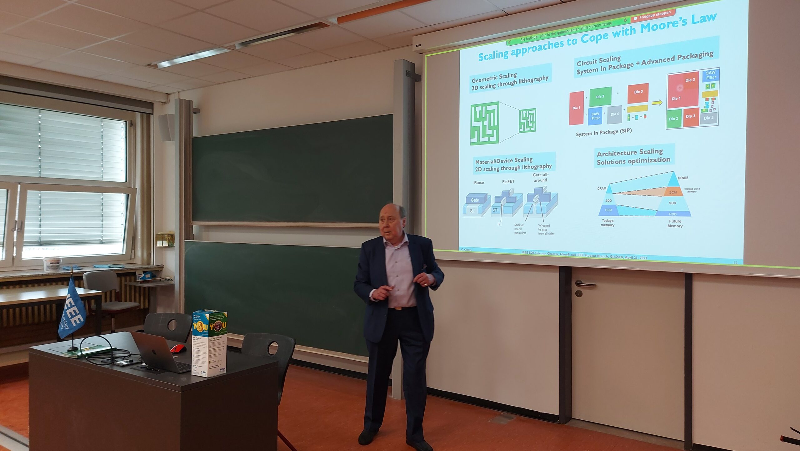
After a warm welcome ofProf.Schwarz, Prof. Claeys started with an evolutionary overview of the microelectronics history. Afterwards, actual numbers and examples of the invests of new waferfabs were given and supported by the evolution of 300mm fabs over the last decades. Prof. Claeys highlighted the different aspects of waferfab investment and it occurring management to make revenue. From that point of view more details in scaling approaches to cope Moore’s Law where presented with its different implications of technology. These focus finally in advance silicon devices from planar FET to Stacked Nanosheet (NS) and approaches like Forksheet (FSH).
Afterwards, Prof.Claeys gave insights in Germanium devices and its most important challenge: Defects. He referred to the stacks of Germanium devices to control defects, gave some examples on the feasibility of Ge-Technology at device level and many famous examples. Then next topic focused on III-V on Silicon with it aspects on lattice mismatch, resulting defects and measures to improves device performances. Many examples of state-of-art devices were given. A comparison was between the progress in GaN and SiC was also discussed.
Prof. Cor Claeys during his lecture 75 Years of the Transistor – Trends and Challenges in Micro- and Nanoelectronics for the Next Decade.
Finally, Prof. Claeys offered the impact of increased system functionality and density achieved by 3D integration based on Through Silicon Vias (TSV) and/or monolithic or 3D sequential integration on a Si substrate. He discussed the evolution, trends and challenges imposed on materials and devices for different integration technologies.