Successful hybrid Benjamin Iniguez DL on “2D Semiconductor FET Modeling”
It felt somehow strange entering a lecture room at THM and introducing Prof. Benjamin Iniguez for the IEEE EDS Distinguished Lecture “2D Semiconductor Modeling” in front of students and staff of the Device Modeling Research Group of NanoP from THM – University of Applied Sciences. Shortly announced, 12 IEEE participants and 8 non IEEE members attended the lecture, where 10 were present at the THM and 10 by Zoom. After almost more than two years of pandemic a portion of normality came back into daily business.
The distinguished lecture was organized by the EDS Germany Chapter and co-sponsored by the NanoP from THM – University of Applied Sciences. Prof. Benjamin Iniguez from University Rovira i Virgili, Spain gave an overview of 2D Semiconductors with the focus set on modeling of those devices. He highlighted different technological and physical aspects and offered modeling approaches of those devices in comparison with experimental data of TU Vienna fabricated by Max Lemme’s group at AMO Aachen, Germany.
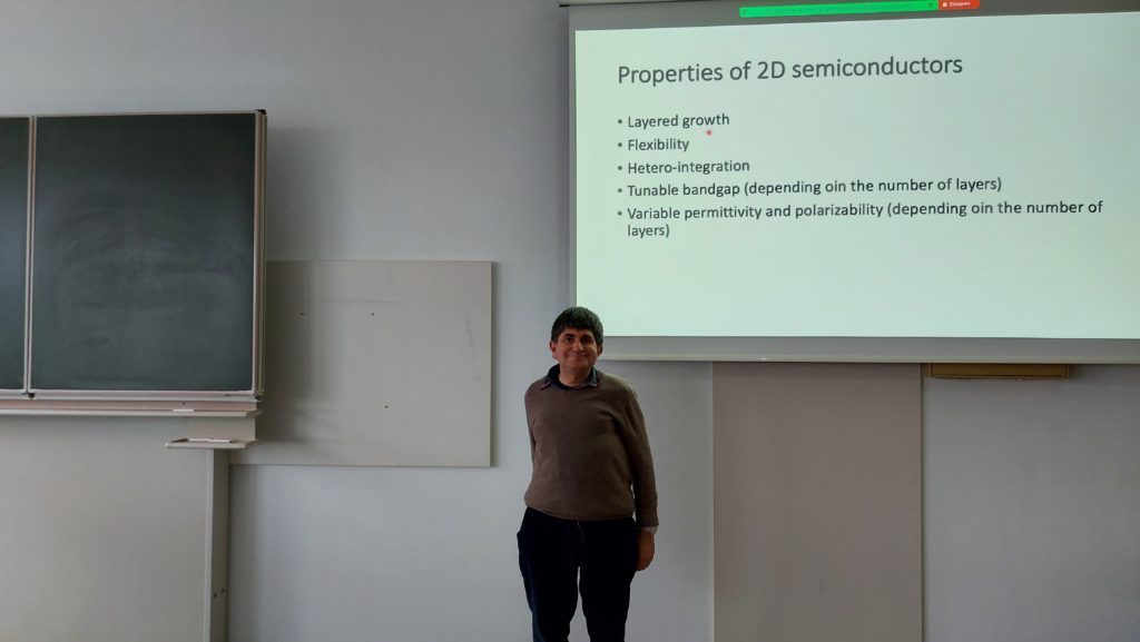
As said, Prof. Iniguez started with an introduction into the topic and properties of 2D semiconductors. The dicussed TMDs (Transition metal dichalcogenide) band structure depending on the layers, gave insights of black phosphorous, and pWSe2 and nMoS2 on Wafer devices. Afterwards, the physical mechanisms related to 2D material devices were reviewed and modeling challenges as 2D charge sheet density, large DOS and large quantum capacitance, interface traps and mobility degradation as well as inefficient source/drain doping were highlighted.
Then he gave focus on the IV curve modeling followed by the CV modeling with a charge control model. Furthermore, he discussed modeling alternatives and presented results in comparison with experimental data. Finally, the talk gave some conclusions. After the lecture a discussion on certain questions from the participants took place.