How to report and benchmark emerging field-effect transistors

One of the challenges encountered by research on novel electronic devices is to compare devices based on different materials in a consistent way.RWTH Professor Max Lemme and colleagues from USA, China, and Belgium have now proposed a set of clear guidelines for benchmarking key parameters and performance metrics of emergent field-effect transistors. The guidelines have been published as a Perspective Article in Nature Electronics.

Research on field-effect transistors (FET) has long exploredthe possibility of replacingsilicon as channel material with emerging nanomaterials, such as carbon nanotubes, graphene, transition metal dichalcogenides,organic semiconductors, or ultrathin oxides. Thefield is thriving and keeps uncovering fundamental aspects of these materials.But when it comes to comparing the performance of different devices, there is often a lack of consistent reporting and benchmarking.

“Assessing consistently the potential of new materialsfor novel transistorsis difficult, because the performance depends on many aspects and details of the device structure, and many parameters are interdependent.” explains Prof. Lemme. Further complexity is addedto the field by the interdisciplinarity of the research community, whichincludes electrical engineers, chemists, materials scientist and physicists. The multitude of approachesincreases the challenge of reporting and benchmarking results consistently.

To address this situation, Lemme and colleagues have prepared a checklist of device parameters to be reported, as well as a list of recommended benchmarking plots to compare device parameters and performance metrics. In addition, they present an explicit example of how to use the proposed procedure by applying it to the case of FETs based on monolayer molybdenum disulfide (MoS2), which is one of the emerging materials most studied in recent years for transistorapplication.

“To identify the real advantages and opportunities offered by novel materials in the search for improved transistors, we needto be able to benchmark and report different devices in a consistent way. We also need to make sure that all relevant data are reported every time.” adds Lemme. “We hope that our work will contribute to bring clarity in the community and guide the search for even better devices.”


Bibliographic info
“How to report and benchmark emerging field-effect transistors”
Z. Cheng, C.-S. Pang, P. Wang, S. T. Le, Y. Wu, D. Shahrjerdi, I. Radu, M. C. Lemme, L.-M. Peng, X. Duan, Z. Chen, J. Appenzeller, S. J. Koester, E. Pop, A. D. Franklin, and C. A. Richter, Nature Electronics5, 416–423 (2022).
DOI: https://doi.org/10.1038/s41928-022-00798-8

6th Symposium on Schottky Barrier MOS (SB-MOS) devices

The 6th Symposium on Schottky Barrier MOS (SB-MOS) deviceswas held on September 8, 2022at the Competence Center for Nanotechnology and Photonics atTHM – University of Applied Sciences. It was organized by the EDS Germany Chapter and co-sponsored by THM. It was attended by approx. 50 participants in hybrid.

After a short welcome of Prof. Kloes with a detailed schedule, the presentations started with Prof. Richard Forbes from University of Surrey (UK). Prof. Forbes referred on “Apparent conceptual oversight in the statistical mechanics of the reverse-biased Schottky junction, and equivalent devices” with fundamental physics on Schottky junctions. He reported what appears to be a fundamental oversight in the basic statistical mechanics of counting transfers of electrons across a boundary between different media. As physicist he encouraged scientists to be precise in their articles in wording on field emission, thermionic emission or more precise thermal emission, etc. This was acknowledged by the participants.

The next talk was given by Prof. Radu Sporea from University of Surreyon the topic “Contact-controlled TFT design addressing barrier-induced limitations”. He offered, that contact-controlled thin-film transistors are able to achieve superior gain,
low-voltage saturation and uniformity performance at the expense of switching speed
and current density. Prof. Sporea showed that conventional TFT-oriented optimization strategies require adaptation when the contact properties dominate causedfrom choices of constructive and operating parameters. He covered them systematically in this talk, alongside new insights into strategies for reducing temperature dependence. After the presentation a lot of discussions took place which allowed for a short coffee break. Discussions were continued during the break.

Prof. Radu Sporea during the discussion on his presentation.

Afterwards, “Prospects of SBMOS for cryogenic applications” by Prof. Laurie Calvet from CNRS (FR) gave very interesting insights of experimental devices based on superconducting Schottky barrier devices also well known as Josephson junctions. She explained the history and challenges and improvements of those junctions targeting quantum computing applications. The participants were very interested and also here a lot of discussion took place after the presentation.

The symposium continued with “SPICE compact modelling of amorphous oxide semiconductor memristive devices for memristive neural network” by Guilherme Carvalho fromUniversidade do Porto (P). The PhD candidate Carvalho presented experimentally fabricated Mo/a-IGZO/Ti/Mo memristors, in which we deposited the IGZO film by RF-magnetron co-sputtering from three binary ceramic targets and the capability of the device electrical characteristics. He fitted the devices with the Dynamic Memdiode Model (DMM) from Prof. Enrique Miranda’s group, which is well suited for the SPICE circuit simulation of hybrid CMOS-memristor circuits. Those results were benchmarked by simulating a single layer perceptron (SLP) circuit while classifying the handwritten images of the MNIST dataset, reaching an accuracy of ~90%.

The session was continued by the work of the PhD candidate Yiyi Yan from Université catholique de Louvain (BE) on the topic of “Hexagonal Boron NitrideMemristorBased on a NanogapSelf-Formed”.Ms. Yan offered detailed process comics of the different steps she applied to manufacture her devices. Those were supported by optical images (TEM, SEM) of important steps, e.g. Pt silicidation or the wet transfer of CVD-grownh-BN sheets. Impressive was the uniformity of the PtSi process as well as the impact of the various steps and changes onto the memristor device performance, which finally led to significant improvements.

After the lunch PhD candidate Christian Römer from THM – University of Applied Sciences (DE) gave some new insight in “Compact Modelling of Injection Current and Channel-Resistance Effects in Reconfigurable Field-Effect Transistors”. Römer showed the problem of describing the current-voltage characteristics of long channel Schottky barrier field-effect transistors. Here, the resistance of the channel must be considered in the characteristics. He showed a closed-form and physics-based compact model that combines a Schottky-barrier injection current with the limiting effect of a channel resistance. The model was compared with experimental data from NamLab and is in an excellent agreement to those.

Afterwards, Prof. Aníbal Pacheco-Sánchez from Universitat Autònoma de Barcelona (ES)continued on the topic of “Schottky barrier characterization of one-dimensional field-effect transistors”. He introduced into the topic and offered a new approach for 1D devices by the Landauer-Büttiker approach, which led him to a 1D LBM (Landauer-Büttiker Model). Prof. Pacheco-Sánchez compared the model with the 3D AEM and offered a lot of results for the extracted Schottky barrier heights. During the discussion afterwards, the experts agreed that this model is helpful by extracting the Schottky barrier height of 1D devices.

The last presentation of the Symposium was given by Prof. Walter Weber from TU Vienna (AT) and entitled “Exploring the novel Al – SixGe1-xSchottky FET system for the realizationof functionality enhanced transistors, optoelectronics and cryo-electronics”. He was referring on activities of the last decades on Silicon-Germanium and Aluminum material systems in microelectronics. Prof. Weber explained, by combining these materials in the form of geometrically confined nanowires and nanosheets new types of junction formation processes have been recently discovered. It has been found that pure Al-Si nanometer-scale system form atomically sharp Schottky, void-free and single crystal heterojunctions through a thermally driven material solid-state exchange reaction. The reliable Al-Si and Al – SixGe1-x nano-junctions have been found to be promising for the realization of runtime reconfigurable transistors (RFET) featuring electrically programmable n- and p-type polarity control due to their near midgap Fermi level pinning behavior. Pure Ge and Ge rich SixGe1-x channels functionality can be further increased to feature tunable negative differential resistance (NDR) that can be exploited for oscillators and enhanced photodetectors. In addition, the high purity of the single-crystal Al formed by exchanging the Ge and SixGe1-xlayers allows superconductivity below the critical temperature of 1.46 K and the observation of supercurrents in Ge providing a promising device platform for cryogenic electronics. As before, also here a lot of discussion took place.

Prof. Laurie Calvet closed the Symposium with some finally remarks, that Schottky barrier junctions offer a wide spectrum of applications.

MiniColloqium on Memristive Devices

The EDS Germany Chapter organized a hybrid MiniColloqium entitled “Memristive Devices” on September 7, 2022. It was held in the timeframe of the 6th Schottky Barrier Symposium on MOS Devices at the Competence Center for Nanotechnology and Photonics (NanoP) of THM – University of Applied Sciences. It was organized by the EDS Germany Chapter and co-sponsored by THM. The MQ was attended by 19 IEEE participants, as well as other non IEEE members.

The organization committee (Prof. Kloes from THM, Prof. Calvet from CNRS, and Prof. Schwarz from THM) made a successful MQ possible and happen by inviting top level experts on various domains of memristive devices. Topics regarding technology towards simulation and modeling were targeted.

After a short welcome of Prof. Schwarz and Prof. Kloes with instructions, the lectures started with Prof. Mario Lanza from KAUST (SA) on the topic “Characterization of materials and devices at the nano/atomic-scale”. Prof. Lanza offered detailed insights on AFM methods and their challenges to be considered during the characterization of memristive materials. After the lecture a long discussion took place on various questions from the participants.

Prof. Benjamin Iniguez introducing TMD memristors. The inset is showing Prof. Lanza during his AFM presentation.

The feedback of both, lecturers and participants was very positive to the organization, which planned for longer timeslots to enable detailed discussion.

After a coffee break the lecture continued by Prof. Enrique Miranda from Universitat Autònoma de Barcelona (ES) with a talk entitled “Compact modeling of memristive devices for neuromorphic computing”. First, Prof. Miranda introduced the newbies/rookies into the topic of memristive devices and went through different aspects and impacts for the compact modeling approaches. He showed details in static and dynamic modeling and its impact on the IV characteristics. Finally, he offered a SPICE compact model which allows or multiple crossbar array circuit simulation. Afterwards, discussion on the aspects, limitations and advantages took place.

The MQ was closed by a talk of Prof. Benjamin Iniguez from Universitat Rovira i Virgili (ES) on “Challenges and solutions in compact modeling of TMD memristors”. He started in his lecture with an introduction and physical mechanisms in TMD memristors. Afterwards, Prof. Iniguez showed and reviewed modeling solutions including results of those. Finally, he gave a conclusion and outlook of the status quo and where further solutions are required.

Afterwards, Prof. Schwarz closed the MQ and thanked all the speakers and participants for being part of this MQ and the contributions. Present attendees met afterwards for dinner in an old castle nearby the university.

Learning From the Brain to Save Energy

Scientists at Forschungszentrum Jülich and RWTH Aachen Universitywant to create a leading international location for neuromorphic AI hardwaretogether with companies from the region.

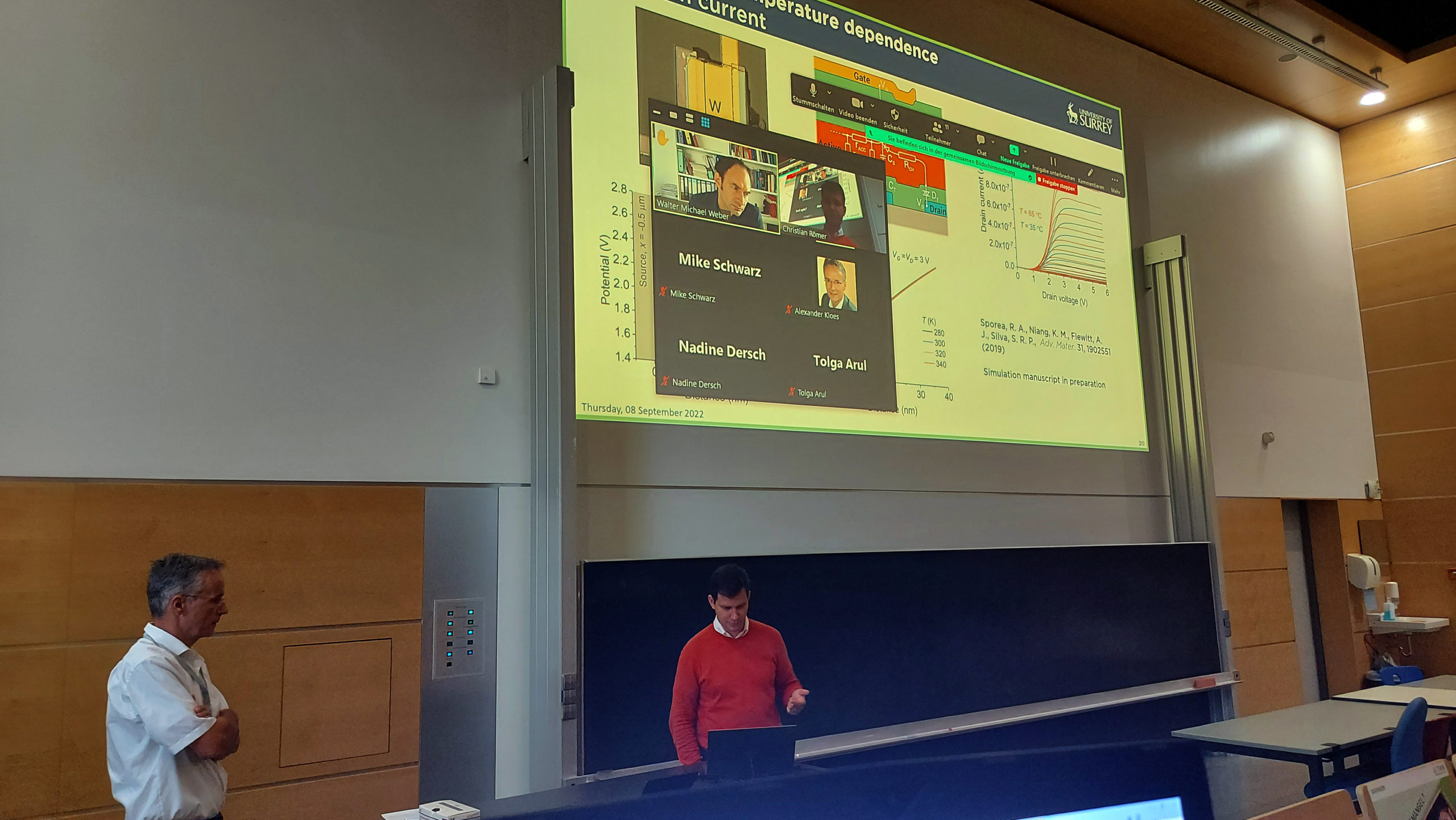
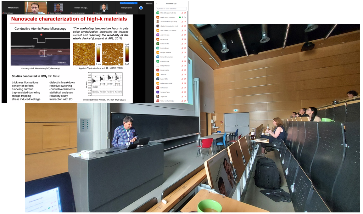
Establishing a technological basis for neuroinspired AI hardware from Europe – that is the goal of the NeuroSys future cluster and the NEUROTEC project, where Forschungszentrum Jülich and RWTH Aachen University are cooperating with each other. To this end, an internationally leading location for neuromorphic hardware – computer chips inspired by the human brain – is to be created in the Jülich-Aachen region in collaboration withlocal high-tech companies. Following a meeting at the Jülich-Aachen Neuromorphic Computing Day, which took place at Forschungszentrum Jülich on May 24, 2022, the researchers are now providing an insight into the interim status of the projects.

NEUROTEC entered its second phase at the end of 2021 and will receive total funding of around 36 million euros over five years from the German Federal Ministry of Education and Research (BMBF). The future cluster “NeuroSys – Neuromorphic Hardware for Autonomous Artificial Intelligence Systems” had prevailed in last year’s Clusters4Future ideas competition and will receive up to 45 million euros in funding from the BMBF.

In this interview, Prof. Rainer Waser of Forschungszentrum Jülich and RWTH Aachen University, coordinator of NEUROTEC (Neuro-inspired Technology of Artificial Intelligence for Future Electronics) together with Prof. Max Christian Lemme of RWTH Aachen University and AMO GmbH, coordinator of the future cluster NeuroSys (Neuromorphic Hardware for Autonomous Systems of Artificial Intelligence) explain the current status of developments.

Prof. Rainer Waser, what exactly do we need such neuromorphic computer chips modeled on the human brain for?

Prof. Rainer Waser: In NEUROTEC, we are focusing on a promising area of the future, namely hardware for artificial intelligence applications. With our approach, we are addressing a very fundamental problem, the energy problem: Because the use of AI is currently still very energy-intensive. The training of models is usually done on supercomputers and requires more and more computing time. Every 3 to 4 months the computational effort doubles, at least this is the trend of the last years.

Neuromorphic systems with artificial synapses promise to solve these tasks much more efficiently – by several orders of magnitude – than is possible with conventional digital computers. In the long term, a wide range of applications is conceivable: from the smallest nanosensors, the “smart dust”, to intelligent implants with energy-autonomous AI control, pattern recognition chips in mobile devices, online-trainable controllers in Industry 4.0, vehicle-based AI electronics for autonomous driving, to mainframe computers that in turn emulate the brain or centrally solve complex AI tasks for the surrounding economy.

The NEUROTEC project is funded by the “Sofortprogramm für den Strukturwandel”. It is intended to help create new jobs in the Rhenish mining region even before the end of coal mining. What exactly do you have in mind?

Prof. Rainer Waser: We plan to support local industry, particularly in the area of basic technologies. The professional sectors that we are addressing extend far beyond actual chip production. This also includes, for example, plant engineering, measurement technology and electronics development. The NEUROTEC II project phase has got off to a very good start since November 2021 and almost all work packages are on schedule. Some work packages are even slightly ahead of their time.

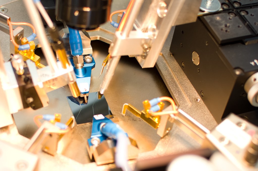
The technology is currently still in the research and development phase. Nevertheless, there are already some initial concrete successes to report. Naturally, these are initially primarily jobs for specialized staff, before the technology matures and the focus shifts to industrial production, when the technology becomes widely used. A current example: Prof. Heuken from AIXTRON SE highlightedat the Jülich-Aachen Neuromorphic Computing Day the prospects that will open up in the next few years in terms of new jobs at AIXTRON in connection with the new 2D materials. These materials are being investigated in the NEUROTEC project for their suitability for neuromorphic computing.

What are the advantages of this neuromorphic hardware you are developing?

Prof. Rainer Waser: Conventional computer chips are based on transistors. We would like to supplement these transistors with a novel memristive component. Such a “resistor with memory” resembles the synapses in natural nerve cells and is therefore particularly suitable for artificial neuronal networks, such as those used for artificial intelligence applications.

An important feature of neuromorphic chips is that computing processes and memory are no longer physically separated. The data transfer between processor and memory that takes place continuously on conventional computers with so-called Von Neumann computer architecture is extremely energy-intensive and slows down computations. In contrast, we envision neuromorphic chips with artificial synapses that can do both: Store information and process it at the same time. Computing is then performed directly in – non-volatile – memory; this is also known as computing-in-memory. And it makes it possible to process information in a highly parallel manner.  The model here is actually the human brain, which requires an average of just 20 Watt. That is several orders of magnitude less than the energy requirements of a supercomputer that performs similar functions using AI.

Prof. Max Christian Lemme, in the NeuroSys future cluster, you are driving forward complementary developments in the field of neuromorphic hardware. The topic is also being intensively pursued globally. Where does the region stand in terms of global competition?

Prof. Max Christian Lemme: The BMBF’s Future Cluster Initiative has the explicit goal of quickly translating excellent cutting-edge research into applications, and doing so in regional alliances. To achieve this, we have brought together researchers along the entire value chain in the NeuroSys future cluster who have worldwide visibility in their respective disciplines. In addition, there are regional companies and start-ups from the high-tech sector. We now cover the entire field from new materials to image and speech processing and medical technology, and expand the concept with socio-economic issues – i.e. research on the ethics of AI, on consequences for the job market and on viable business models for “AI Hardware Made in Europe”.

An advisory board of scientists and international companies completes the cluster. So, I dare to say that we are on par with the global competition. What is missing in the region is a modern semiconductor factory for AI chips, the location of which we have formulated in our vision. With the excellently trained engineers and scientists in the region, including Belgium, the Netherlands and the Ruhr area, the proximity to the research institute IMEC in Belgium and the leading manufacturer of lithography equipment ASML in the Netherlands, we have an excellent argument.

How far has the technology come?

Prof. Max Christian Lemme: As is often the case, there is no simple answer. It is already possible to produce special neuromorphic chips using conventional technology. However, these are still far from the energy efficiency of the brain. Here, the new technologies from resistive switching oxides, phase change materials or even 2D materials can take us much further. However, their use is always a question of industrial manufacturability. This varies from material to material, and it currently looks as if each generation of new materials will also bring a boost in efficiency. It is therefore very important to already be working closely on the two projects with manufacturers of material deposition systems such as Aixtron from Herzogenrath or deep tech start-ups such as Black Semiconductor or Aixscale Photonics.

In parallel, however, the Future Cluster is also working with industry at the higher levels of the value chain. Here, there are several start-ups in the region such as Clinomic Medical, Gremse-IT or a company co-founded by my RWTH Aachen colleague Prof. Rainer Leupers shortly after the NeuroSys launch. So, we are already working on all technology levels to realize the goals and are still in the acceleration phase after an excellent flying start!


More information:

www.neurotec.org

https://www.neurosys.info

Peter Grünberg Institut, Elektronische Materialien (PGI-7)

Forschungsschwerpunkt Neuromorphes Computing

https://www.eld.rwth-aachen.de/go/id/psfz/

Video: https://www.youtube.com/watch?v=tJghcXPby48


Contactperson:

Prof. Dr. Rainer Waser
Koordinator NEUROTEC, Peter Grünberg Institut für Elektronische Materialien (PGI-7), Forschungszentrum Jülich
Tel: 02461 61-5811
E-Mail: r.waser@fz-juelich.de

Prof. Dr. Ing. Max C. Lemme
Koordinator NeuroSys, Lehrstuhl für Elektronische Bauelemente, RWTH Aachen University
Tel: 0241 80 20280
Email:  neurosys@eld.rwth-aachen.de


Media contact:

Dr. Regine Panknin
Unternehmenskommunikation
Tel.: 02461 61-9054
E-Mail: r.panknin@fz-juelich.de

HealingAchilles heel of two-dimensional transistors

Stability – in the sense of stable operation thorough lifetime – is one of the key characteristics that an electronic device need to present to be suitable for applications. And it is the Achilles heel of transistors based on two-dimensional materials, which typically show much worse stability than devices based on silicon. A team of researchers from TU Wien, AMO GmbH, RWTH Aachen University and Wuppertal University has now demonstrated a novel engineering approach to enhance the electrical stability of two-dimensional transistors by carefully tuning the Fermi energy. The results have been reported in Nature Electronics.

Today, there is little doubt that devices based on graphene and other two-dimensional (2D) materials can exceed the state of the art for certain applications, thanks to their intrinsic properties. Two-dimensional materials are also seen as some of the most promising candidates for realizing ultimately scaled transistors at the end of the roadmap of silicon technology.  However, devices based on 2D materials often show poor electrical stability, meaning that their behavior changes depending on their operation history.

“Component reliability is one aspect that is often neglected in research. This is precisely where we have been working for several years, because it is of central importance for applications.” explains Professor Max Lemme, scientific director of AMO GmbH and Head of the Chair of Electronic Devices at RWTH. The instabilityis not only caused by 2D materials themselves, butmostlyby charges trapped into the oxide-insulator used to fabricate the transistors.”Ideally, one would like to use a different insulator with fewer charge traps,” says Lemme, “but there are no scalable solutions for this yet. In our work, we have shown instead that it is possible to use a standard insulator such as aluminum oxide and to significantly suppress the adverse effects of the charge traps in the oxide, by adjusting the charge carrier density in the 2D material.”

The work combines a thorough theoretical analysis of the novel approach – dubbed by the authors ‘stability-based design’ – and a proof of principle demonstration of the concept, performed by measuring different types of graphene-based FETs. The key idea of theapproach is to try to engineer the combination 2D-material/insulator in such a way that the energy of the charge traps in the insulator is as different as possible from the one of the charge carriers in the 2D material. Lemme explains: “Graphene based FETs were the ideal test bed for our approach, as it is relatively easy to tune the energy of charge carriers in graphene. The approach, however, is applicable to all FETs based on 2D semiconductors”.These results represent a major step forward towards stable and reliable 2D materials transistors to be integrated in semiconductor technology.

Bibliographic information:
T. Knobloch, B. Uzlu, Y. Yu. I.llarionov, Z. Wang, M. Otto, L. Filipovic, M. Waltl, D. Neumaier, M. C. Lemme, T. Grasser, Improving stability in two-dimensional transistors with amorphous gate oxides by Fermi-level tuning, Nature Electronics (2022)– Open Access
DOI:10.1038/s41928-022-00768-0

Contact:
Prof. Max C. Lemme
AMO GmbH
lemme@amo.de