7th Symposium on Schottky Barrier MOS (SB-MOS) devices – The Schottky barrier transistor in emerging electronic devices
The 7th Symposium on Schottky Barrier MOS (SB-MOS) devices was held on September 28/29, 2023 at the Ecole Polytechnique in Palaiseau. It was a joint chapter event organized by the EDS France and Germany Chapter and co-sponsored by Ecole Polytechnique and CNRS. It was attended by approx. 30 participants in presence and hybrid format.
After a short welcome of Dr. Laurie Calvet from CNRS-Ecole Polytechnique (FR) with a detailed schedule, the presentations were started by the chair Kham Niang with an inspiring talk of Dr. Calvet on the topic of “The Schottky barrier transistor in emerging electronic devices”. She reviewed the variety of applications and material systems for over 60 years and introduced the SB transistor. She started with an overview of the device modeling and presented the two large classes of SB devices: 1) those that aim to reduce the Schottky barrier and 2) those that aim to take advantage of it. The talk concluded with a series of questions meant to serve as the starting point for the panel discussion later in the afternoon.
The next talk entitled “Silicon-Germanium Nanosheet Schottky FETs, from Contact Properties to Runtime Reconfigurable Circuit Demonstrators” was given by Prof. Walter Weber, TU Vienna (AT). Prof. Weber offered new insights of Silicon germanium (SixGe1-x). While the Silicon germanium (SixGe1-x) active regions have been intensively investigated for the realization of both bipolar and field effect devices over the past decades, the realization of ultrathin-body SixGe1-x transistors, in particular Schottky contact transistors, with high germanium channel content has been hampered by instabilities of the semiconductor interfaces towards metals and insulators. Prof. Weber discussed the combination of advances in ultra-low-temperature epitaxy, contact- and interface- solid state Al diffusion processes as well as reliable surface passivation measures that allow for the realization of ultrathin SixGe1-xnanosheet Schottky contact FETs being integrated on commercially available silicon-on-insulator substrates. He offered high resolution images of the obtained Schottky SixGe1-x devices with abrupt Al contacts which form a base technology for the realization of future contenders of electronic devices beyond the scope of the industrial roadmaps that profit from the abrupt Schottky junctions and high germanium content. Finally, Prof. Weber showed the possibilities to runtime reconfigurable transistors, neuromorphic devices and cryogenic quantum devices can be realized from the same technological platform.
The symposium continued with “DC Compact Modeling of Schottky Barrier Field-Effect Transistors at Deep Cryogenic Temperatures”. The PhD candidate Christian Römer from THM (DE) discussed Schottky barrier field-effect transistors as candidates for applications at cryogenic temperatures, since its characteristics improve with decreasing temperatures. He presented a physics-based DC compact model to calculate the injection tunneling current through a device’s Schottky barrier. A verification of the compact model was performed by measurements at temperatures around 5 K.
The final part of the first workshop day was the panel discussion on the question “What is the future of Schottky barrier devices?”. At the panel Dr. Calvet, Prof. Weber and PhD candidate Römer offered their opinion and various questions we discussed from different aspects.
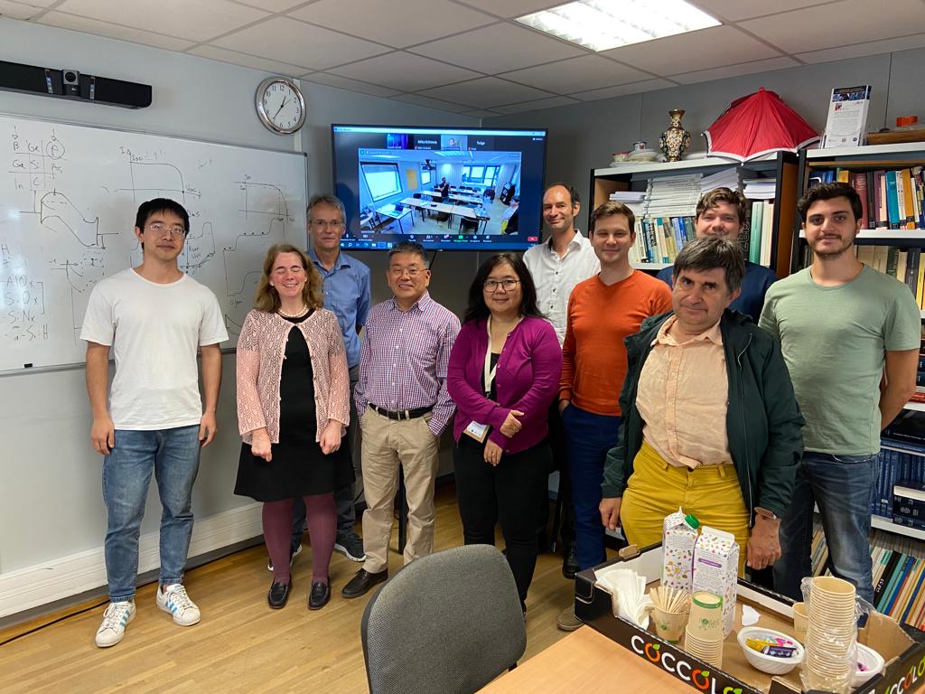
Participants of the 7th Symposium on Schottky Barrier MOS (SB-MOS) devices.
The second workshop day was chaired by Prof. Weber and started with the talk entitled “Ferroelectric Schottky barrier transistor for neuromorphic computing” by Prof. Qing-Tai Zhao from the Forschungszentrum Jülich (DE). Prof. Zhao offered the challenges of the slow and ambipolar switching behavior of Schottky barrier MOSFETs which poses certain challenges for logic applications. Nevertheless, during his presentation he explored its potential application in neuromorphic computing when combined with a ferroelectric gate oxide. Prof. Zhao discussed the implementation of artificial synapses and capacitorless neurons using ferroelectric Schottky barrier transistors. By this novel approach he offered advantages for advancing the field of neuromorphic computing.
The next talk was given by Prof. Radu Sporea from University of Surrey (UK). Before he started with the talk of “Recent implementations of source-gated transistors and circuits with high gain”, Prof. Sporea shortly introduced the campus of Surrey where the next Symposium of Schottky Barrier MOS devices will take place. Then he continued with the source-gated transistor (SGT), which one is celebrating 20 years since its invention and presented that some of the more fundamental limitations of these devices have been explored and gradually overcome. The latest advances in exploiting the SGT’s high intrinsic gain, along with a roundup of essential design rules of thumb were offered.
Afterwards, Prof. Alexander Kloes from THM (DE) presented “Evaluation of approaches for analytical calculation of tunneling currents in Schottky barrier transistors”. He explained the different methods to calculate the transmission coefficient in the tunneling equation, explaining why compact modeling of tunneling currents is so challenging. Prof. Kloes reviewed the analytical calculation of a quantum wave based current transport through Schottky barriers that are suitable for compact modeling. He focused on a new promising approach based on the wavelet transform.
“Indium Gallium Zinc Oxide Source-Gated Transistors” by PhD candidate Kham Niang of University of Cambridge (UK) was the next talk. She discussed the use of amorphous oxide semiconductor (AOS) thin film transistors (TFTs)as SGTs. She presented the fabrication and performance of recent IGZO SGTs and discussed in particular the challenges in realizing a Schottky contact between AOS and high work function metal, and presented various methods adopted to mitigate this problem.
The presentations continued with “TCAD simulation studies of source-gated p-type CuO TFTs” by PhD candidate Qi Chen from the Université catholique de Louvain (UCLouvain) (BE). Source-gated p-type CuO TFTs with HfO2 gate dielectric were studied using TCAD tools. Based on parameters extracted from experiments, the gate modulation of the source barrier was investigated varying the thicknesses of CuO and HfO2 and the Schottky barrier height at the source contact. The optimal structure design was further explored to obtain good transconductance and output conductance parameters for circuit design.
Afterwards Prof. Benjamin Iniguez from URV (ES) gave a talk entitled “Compact modeling of the nonlinear contact effects in Organic Thin Film Transistors”. He presented the nonlinear contact effects due to the presence of Schottky barrier at the source-channel interface which may significantly affect the I-V characteristics in Organic Thin Film Transistors. He reviewed four different models that can be used for compact modeling.
The final talk was given by PhD candidate Patryk Golec from University of Surrey (UK). His talk on “A Source-Gated Transistor Compact Model Designed Using TCAD Simulations” offered a compact model developed for a source gated transistor (SGT) using the data obtained from TCAD simulation. He made some fundamental simulation to explain the fundamental different current injection mechanism occurring at the source region. This causes the contact effects to be dominant in the SGT, as opposed to the TFT. With this the resulting compact model of an a-Si SGT describes the changes in device parameters within the source region.
Dr. Laurie Calvet closed the Symposium with some finally remarks, that Schottky barrier junctions offer a wide spectrum of applications and thanked all participants and organizers for realizing this SSBMOS.