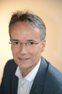
Name:
Prof. Alexander Kloes
University & Institute:
TH Mittelhessen – University of Applied Sciences
Competence Center for Nanotechnology and Photonics (NanoP)
Wiesenstrasse 14, 35390 Giessen
(go.thm.de/dmrg)
Biography:
Alexander Kloes (M’95–SM’16) received the Diploma and Ph.D. degrees in electrical engineering from the Solid-State Electronics Laboratory, Technical University of Darmstadt, Darmstadt, Germany, in 1993 and 1997, respectively.
Since 2002, he has been a Professor with the TH Mittelhessen University of Applied Sciences, Giessen, Germany. His current research interests include modeling of semiconductor devices, especially for nanoscale MOS devices and organic TFTs.
Volunteer Position within EDS:
reviewer for TED, EDL, JEDS
Email:
alexander.kloes@ei.thm.de
Google Scholar:
https://scholar.google.com/citations?hl=de&user=vLMQS2gAAAAJ
Orcid:
https://orcid.org/0000-0002-6485-1512
Expertise:
Electronic devices, physics based modeling and TCAD simulation, digital signal processing
Research Interests:
Compact modeling and TCAD simulation of nanoscale transistors, organic thin-film transistors, memristors
(Public) Research Labs:
Waferprober incl. B1500 parameter analyzer
DIMATIX material printer DMP-2831
Simulation software: TCAD Sentaurus, QuantumATK, Cadence Design Framework
